MX2 Semi-Conductor Monolayers, Cubed


wikiTransition Metal Dichalcogenide Monolayers (TMD)
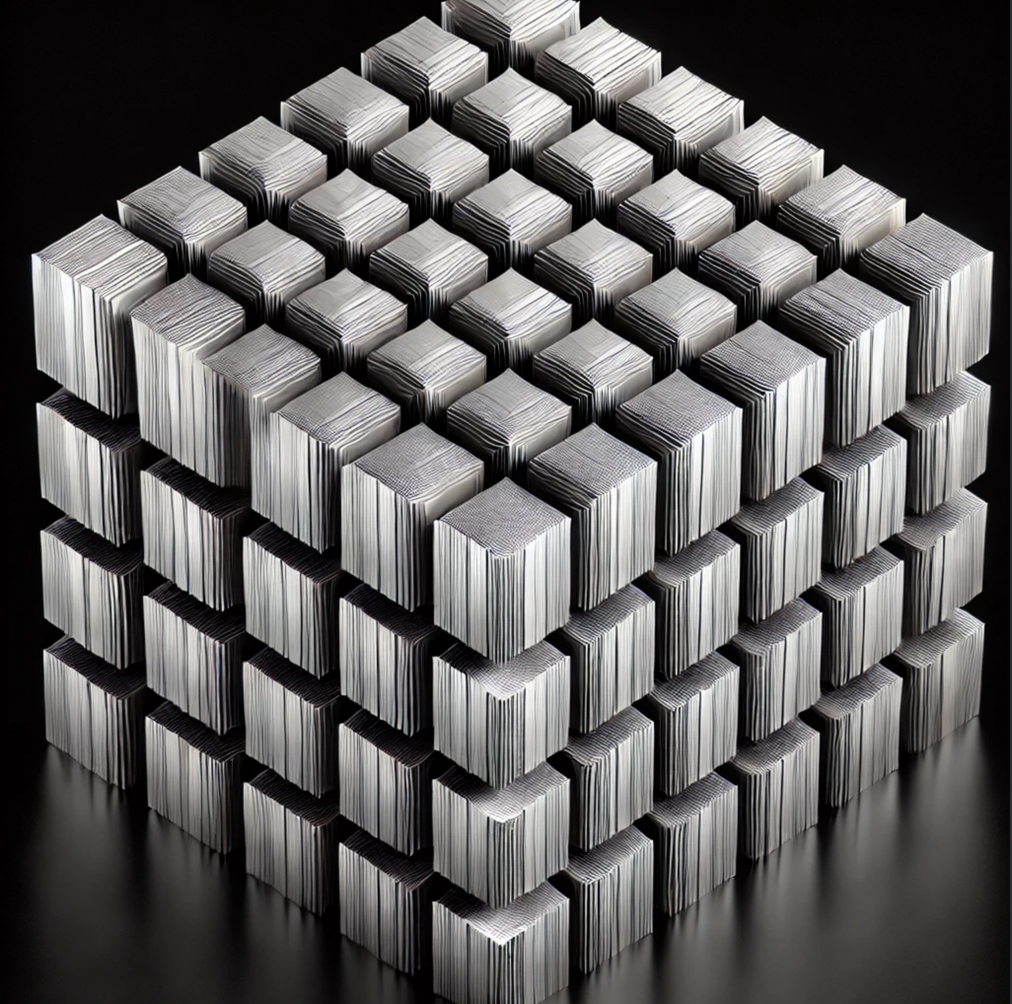
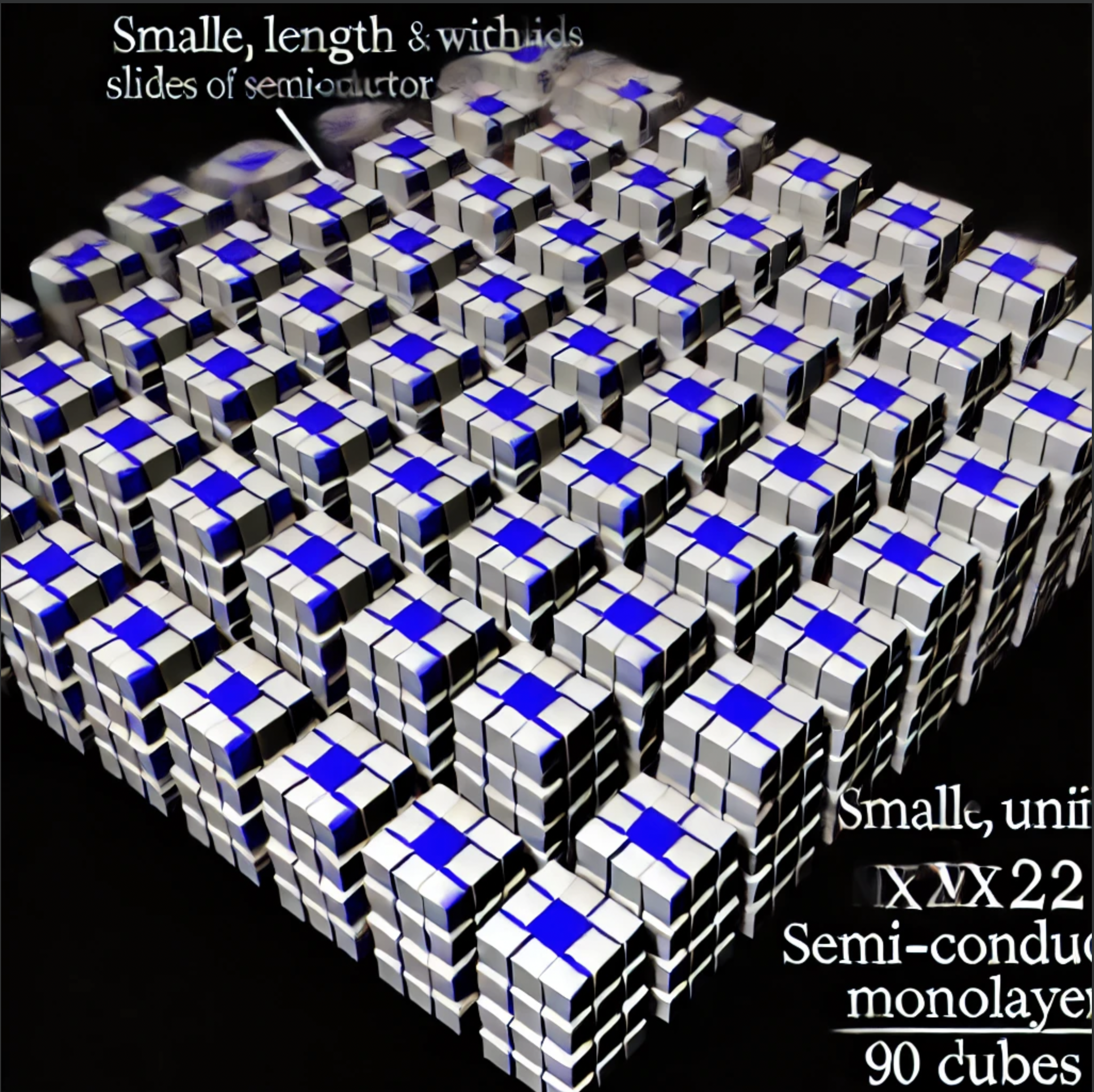
In stacking monolayers into cubed patterns, perhaps rotating cubes for an equality of balancing material properties (isotropy). An example monolayer being 6.5 Å thick (MoS2). With activation potentials being proxy based the right lightware language could balance the gap charges required for initialization and tuning.

Utilizing lightware, to adjust the light intensity, wavelength, or polarization in real-time to tune the electronic properties of the MX2 stacks according to specific needs.

Benefits
- Photonics and Optoelectronics: This configuration could be particularly useful in photonics and optoelectronics, where precise control over light-matter interaction is essential.
- Computational Materials: For computational applications, this setup could allow for the development of highly efficient, light-controlled logic devices or memory storage systems.
- Dynamic Sensors and Actuators: In sensors and actuators, the ability to rapidly modify material properties via light could lead to highly sensitive and responsive systems, adaptable to varying conditions without physical contact or mechanical adjustments.
Application
Electroplating is known to work in creating MX2 monolayers. A miniature ensemble for theoretical conveyer belts of self growing 'lamp socks' with the right programmer of the science of lightware and zyphers.
Atom Lasers and Material Dynamics
Atom lasers are at the forefront of material science innovation, offering unparalleled precision in modifying MX2 lattices. By utilizing coherent atomic streams, these lasers enable dynamic adjustments to material properties, making them ideal for advanced energy applications and structural enhancements.
Interaction with MX2 Lattices
MX2 lattices, known for their unique 2D properties and high conductivity, gain enhanced functionality when coupled with atom lasers:
- Precise Energy Transfers: Atom lasers facilitate localized energy deposition, optimizing lattice conductivity and efficiency.
- Structural Modifications: The coherent nature of atomic streams allows for real-time reconfiguration of lattice bonds, enabling adaptive materials.
- Enhanced Stability: MX2 lattices achieve greater resilience through atom laser-induced adjustments to bond angles and electronic properties.
Applications in Advanced Materials
The integration of atom lasers with MX2 lattices paves the way for innovative applications:
- Next-Gen Energy Systems: Developing ultra-efficient energy storage and transfer systems through atomically precise lattice engineering.
- Adaptive Surfaces: Creating materials that respond to environmental stimuli, such as temperature or pressure changes, with atom-laser-guided adjustments.
- Quantum Computing: Leveraging enhanced MX2 lattices for improved qubit coherence and stability in quantum devices.
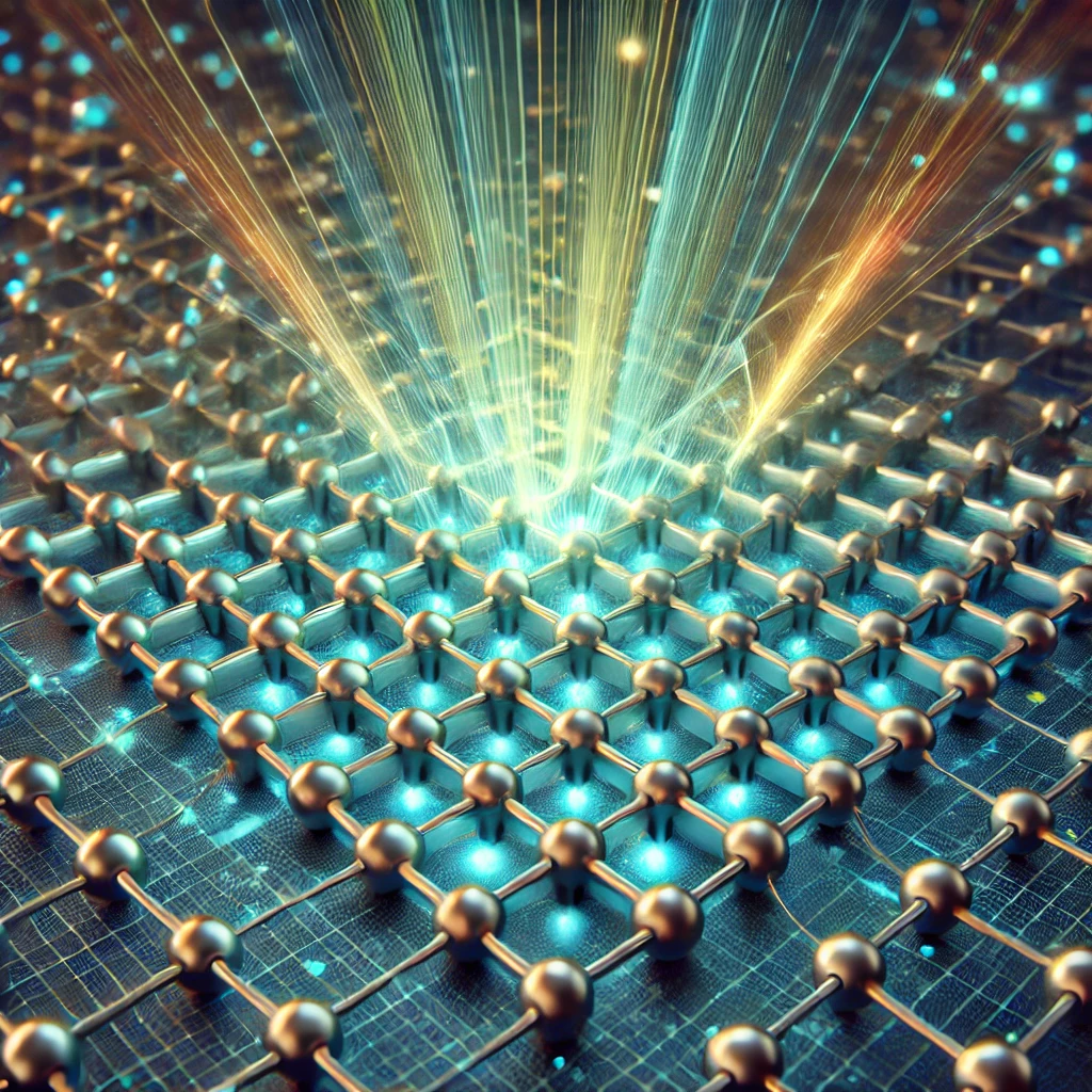
Visualization of Atom Laser Interaction
Imagine a 2D MX2 lattice illuminated by atom lasers, where coherent atomic streams align lattice bonds for precise energy transfers and dynamic material adjustments.

Future Potential
As atom laser technology advances, their integration with MX2 lattices will enable breakthroughs in fields such as:
- Nanotechnology: Designing self-healing materials with atomically controlled precision.
- Energy Harvesting: Enhancing lattice performance for renewable energy systems.
- Space Exploration: Developing lightweight, adaptive materials for spacecraft and habitats.
<= Back
<= Home (Splash)